
A week ago I’ve received a ping from my CEO invinting me to join a meeting. No clue about the meeting’s subject nor the attendants. But an hour later, here I am joining a call with Gautier Soubrane and Maxime Portaz from Graphcore, delving into a topic entirely unfamiliar to me: IPUs.
This meeting really piqued my curiosity. What in the world are IPUs? How are they different from CPUs or GPUs? And what on earth are they used for?
After diving into the subject for hours, I decided to whip up a brief summary to unravel the mystery of what the heck an IPU is.
What’s an IPU
So, let’s break it down: What exactly is this IPU thing? Well, IPU stands for Intelligence Processing Unit, and you can think of it as a fusion between a CPU and a GPU, but with a special focus on the needs of machine learning.
Picture this: more memory and more cores than your typical CPU and snappier arithmetic skills than your run-of-the-mill GPU – that’s the IPU. The IPU is all about delivering top-notch performance for those intricate operations spread out across a high number of threads (which basically means that it can handle tasks across its “cores” and memory efficiently, even if they’re scattered all over the place).
Who’s behind it
So, who’s the brainpower behind this IPU innovation? Well, it all started back in 2013 when two fellas, Simon Knowles and Nigel Toon, kickstarted Graphcore. Honestly, I had never heard of them or their previous ventures before this adventure, but hey, we’re all in the learning boat together here. (And if you’re a hardware whiz, feel free to drop some knowledge my way!)
Fast forward three years, and Graphcore officially becomes a company. In the same year, they manage to bag a cool $32 million in a Series A funding round, with one of the venture capitalists being Foundation Capital, the same folks who’ve also got their fingers in the pies of Solana (seed round) and Netflix (C/D/E rounds). Now, that’s seriously impressive.
Graphcore’s growth train keeps chugging along, with more cash injections through subsequent funding rounds, and even big names like Sequoia hop on board during the C round.
The first IPU made its debut in 2018 and is avaible on the Azure cloud since 20191. Fast forward to 2023, and Graphcore is now a multi-billion-dollar powerhouse with over 500+ employees spread out across the globe.
TL;DR: These guys aren’t tinkering with random gadgets in their garage, that’s for sure!
How does that work
Now place to my favorite section! How does an IPU works and what’s it’s design?
⚠️ disclaimer:I’m not an hardware engineer so I’ll do my best to break it down for you. And if any hardware gurus are lurking around, feel free to jump in and share some knowledge
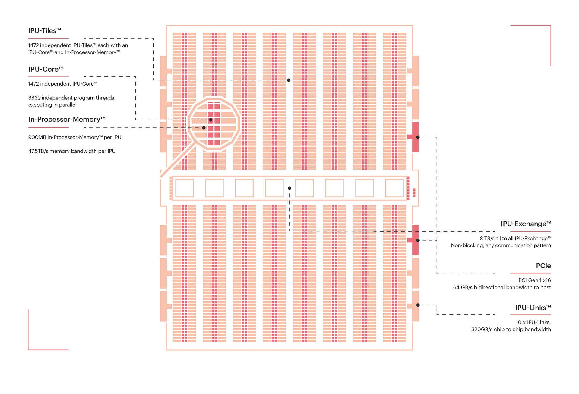
An IPU is like a puzzle made up of four key pieces: Tiles, Exchange, IPU-Links and PCIe. Let’s dive into the workding of each of those four components.
Tiles
An IPU consists of over a thousand tiles (1472 in the MK2 and MK2X2 versions and 1216 for the MK1), and these tiles are responsible for both performing arithmetic operations and storing data.
Each tile consists of two primary components: a “core” and its local SRAM memory (256kb per tile for the MK1 and 624kb for the MK2). These two components work together in harmony. The ingenious part of this design is that each IPU core is powerful enough to execute entirely different programs while having rapid access to a significant amount of memory.
Here’s where it gets interesting: There are no caches, no physical global memory – just IPU cores and their local memories. This is what allows IPUs to handle sparse data loads without a hit to performance. Imagine, this is quite a departure from the way GPUs utilize multiple cache layers or how CPUs rely on very small registers and need to interact with RAM.
As for the inner workings of the IPU-Core itself, I won’t delve too deeply into the details (this is IPU-101, after all), but here are a few key things to know:
Each IPU-Core has the capability to execute 6 threads. Most worker instructions take just one compute cycle to execute, except for memory access, which requires six clock cycles. This latency is fixed and doesn’t depend on access patterns, stride, or global workload.
Threads can be executed in two modes: supervisor and worker. An IPU-Core can have at most one supervisor thread at a time. This supervisor thread runs the top-level control program of its Tile and can spawn other threads that will run in worker mode. These “worker” threads execute the user’s program and, when completed, exit to allow the supervisor to spawn a new worker thread. Note that the supervisor thread can still spawn a worker thread when none are available; it will suspend itself and be used for a worker task.
Exchange
So, we’ve got these tiles, each with its own IPU-Core and memory. But what happens when you need these tiles to communicate or share data across boundaries? That’s where the Exchange comes into the picture. Think of it as an on-chip interconnect that enables high-bandwidth communication between tiles.
Alright, tiles can talk to each other, but why is this such a big deal? Well, it changes everything. Now, those sets of SRAM aren’t independent anymore; they work together as a single global memory! Instead of having 1472 x 624kb of memory, you’ve effectively got 918Mb at your disposal! Some might argue that it still falls short compared to the VRAM in a high-end GPU which boasts around ~80Gb, but here’s where I’d counter that it’s like comparing apples and oranges (don’t worry, I made the same mistake).
To understand why GPU’s VRAM cannot be compared with IPU’s SRAM we need to dive a bit into their purposes and inner working.
A GPU relies on a complex Memory Hierarchy system and multiple cache layers to choreograph data, with VRAM being the cavernous storage often hailed. However, crucially, not all operations waltz through VRAM; that’s the job of the L1 cache, which takes center stage in direct communion with the SMs (Streaming Multiprocessors). VRAM essentially plays the role of an easily accessible data vault.
On the flip side, the SRAM blocks in IPUs are soulmates with their respective tiles. There’s no buffer zone between the tiles and their memory blocks. So, is it akin to a cache? Well, not quite. While caches are often painted as “a component that stores data so that future requests for that data can be served faster” the SRAM in an IPU isn’t a transient pit stop to expedite data access; it’s the chief data depot for the entire chip.
Now, you see why equating GPU VRAM and IPU SRAM is a bit like comparing apples to oranges, and if you need to store more data you can always use some regular DRAM (at the expense of speed).

IPU-Links
Now, let’s think bigger. What if I told you that you can connect multiple IPUs together to create a super-IPU? Well, that’s precisely the job of IPU-Links (10 per IPU). IPU-Links enable off-chip communication, albeit at a lower bandwidth.
Graphcore’s engineers have made it a priority to make data transfers between remote tiles (off-chip) just as straightforward for programmers as those between local tiles (on-chip). This paves the way for high scalability. Essentially, the idea is this: Need more memory or compute power? Just add more IPUs. (The MK1 supports up to 4096 interconnected IPUs!)

PCIe
Finally, we have PCIe Express (two per IPU) for host connectivity. Keep in mind that this is the slowest option for data transfer, so it should be used sparingly, or you’ll incur a hit to throughput.
Bulk Synchronous Parallel Model (BSP)
If you’re anything like me and the concept of BSP is brand new to you, it’s time to embark on a journey into the algorithmic side of IPUs. To make efficient and secure computations and communications across its tiles, Graphcore has embraced the Bulk Synchronous Parallel Model.
Here’s the “simple” idea, each tile carries out computations in what are called supersteps, consisting of three distinct phases:
- Exchange: Data is moved from and to the tiles
- Compute: Arithmetic is computed on the IPU-Core
- Sync: A synchronization phase is done, nothing happens on the tile until every other tiles of the IPU reach this point
This loop is then repeated until end of the execution.

Seems straightforward, right? Well, here’s the kicker: BSP isn’t just a software trick applied to the IPU; the hardware itself is designed in harmony with this model! Tiles can only directly access their local memory, which enforces the compute phase. Meanwhile, the Exchange step takes charge of synchronizing and facilitating communication.
Conclusion
Now, you might be wondering, with IPUs offering such impressive technology, why aren’t we making a mad rush to replace all our hardware with them?
As is often the case, the answer to this question is multifaceted, but one of the main reasons boils down to convenience.
As ML engineers, we’re accustomed to having access to large amounts of swiftly accessible memory, often in the tens of gigabytes range. While IPUs do provide a substantial amount of storage and can still utilize regular DRAM, it often falls short of our current needs. Gautier S. kindly explained to me that Graphcore believes the strategy of relying on ever-larger VRAM each year isn’t sustainable. High Bandwidth Memory (HBM), which is used in GPUs for their massive VRAM, is prohibitively expensive, and this pricing trajectory would be challenging for consumers to keep up with. Graphcore encourages us to optimize the memory usage of our models and algorithms, which is why they’ve chosen not to go the HBM route.
Which leads me to the other significant factor: versatility. While a GPU can handle almost every ML task, including training, fine-tuning, and inference, an IPU may encounter difficulties with inference due to its memory limitations. During the fine-tuning of a large model (> 1 Gb), you can imagine loading and unloading parts of your model as you backpropagate gradients. However, for inference, unloading parts of you model would result in a significant drop in throughput and an increase in latency, which may not align with production requirements. On the other hand, for relatively small models like BERT, an IPU can serve well for inference. This brings us back to Graphcore’s belief that we can’t simply scale to very large models and expect hardware memory to scale in lockstep, and should instead take the needed time to optimize our model and their memory footprint.
As long as IPUs contend with these memory constraints, it’s challenging for me to envision the market shifting decisively towards them. Start-ups want hardware that’s easy to use and versatile, and cloud providers aim to provide what their customers demand. However, IPUs might be an excellent fit for specialized companies with specific needs. And who knows what the future holds? Perhaps one day, I’ll find myself preferring an IPU MK4 over an H100. Either way, having competition against the juggernaut that NVIDIA has become is always a good thing.
There’s plenty more to explore when it comes to how IPUs function, their core functionality, memory management, software integration, and the world of IPUs in general. If your curiosity is piqued and you’re itching to learn more, here are a few resources I highly recommend:
- IPU programmer’s guide
- IPU’s Memory performance optimisation
- Dissecting the Graphcore IPU Architecture via Microbenchmarking
- Scalable Machine Intelligence Systems: Graphcore SVP Software Matt Fyles at ISC2020
- TPU vs GPU vs Cerebras vs Graphcore: A Fair Comparison between ML Hardware
I genuinely hope you enjoyed this brief blog post about IPUs, and I’d greatly appreciate any feedback you’d like to share. I know I can’t make everyone happy, but I’m sincerely eager to learn how I can enhance my writing.
Lastly, a big thank you to Gautier S. and Maxime P. from Graphcore, who kindly took the time to explain some intricacies of their hardware and validate the technical aspects of this blog post while respecting my personal opinions.
-
It seems that IPUs are no-longer available on Azure (not so profitable?) and are now accessible via GCore and PaperSpace. ↩︎
-
Updates done to the MK2 leading to the creating of the MK2X are pretty interesting and would require a full dedicated blog post. ↩︎